Hello and welcome to the electronic circuits for beginners' electronics course!
This course was originally designed for an intensive classroom course, but has been adapted to the online format for all of you to study. It covers everything from basic electronic physics to basic components and all the way to digital electronics.
Quadrocopters, also known and quadrotors, are one of the most interesting little flying machines ever imagined; yet there's a load of disperse and almost undecipherable amount of information that comes from hobbyists' and builder's gut feeling on what seems to be the right thing to do.
This is my attempt at bringing all that information together in a simple to understand version for beginners to get designing their own quadrotors.
How they work
Quadrotor diagram showing forces and torques
The concept is a flying machine with four motors aligned in a square; two on opposite sides of the square rotate in one direction and the other two rotate in the opposite direction.
This four rotor helicopter gives us some interesting properties:
1.- each motor lifts only a quarter of the weight of the heli, so we can potentially use less powerful motors
2.- the rotation or torque of the first pair of motors is canceled by the rotation of the second pair that goes in the opposite direction. Let me explain how this works:
On a regular helicopter, you have one big rotor to provide the lifting power and a little tail rotor; this one counteracts the rotation that the main big rotor would otherwise pass on to the structure of the helicopter (making it rotate almost as fast as the propeller)
On a quadrotor, if all motors turned on the same direction the thing would rotate same as a regular heli without tail rotor; the clever thing is that since one pair create a torque or rotation on one direction, the motors turning on the opposite direction create a torque also but on the opposite direction. These torques tend to cancel out and the quadrocopter stays facing the same direction without any rolling around.
Quadrotor control; arrow thickness denotes power
3.- control becomes a matter of which motor gets more power and which one gets less.
Yaw (where the thing is "facing"; using your head, yaw is when turning left and right) is controlled by turning up the speed of the regular rotating motors and taking away power from the counter rotating; by taking away the same amount that you put in on the regular rotors produces no extra lift (it won't go higher) but since the counter torque is now less, the quadrotor rotates as explained earlier.
Roll (how tilted to the side it is while still facing the same direction; using your head, roll is turning it so that your chin is parallel to the ground) is controlled by increasing speed on one motor and lowering on the opposite one.
Pitch (how tilted it is; using your head is moving it up and down, similar to nodding) is controlled the same way as roll, but using the second set of motors. This may be kinda confusing, but roll and pitch are determined from where the "front" of the thing is, and in a quadrotor they are basically interchangeable; but do take note that you have to decide which way is front and be consistent or your control may go out of control.
These three can be controlled at the same time to give all the range of motion you could ever need from a flying thing
Now, building and flying a quadrotor from a remote control is simple and fun and stuff, but people noting the inherently stable flight (in theory with equal speed of the motors the thing keeps itself level) and ease of control (only three functions and they are all basically take speed from one and put in the other), people love to make them autonomous (flies itself) and semi-autonomous (at least keeps itself level by responding to disturbances and error).
Common sensors (Gyro, Accelerometer, Sonar/Rangefinder)
A gyroscope is a device that tells you the difference in angle from a reference one: this is useful in keeping the quadrocopter level so it won't fall or go sideways when we don't want it to.
Micro ElectroMechanic Mechanism (MEMS) gyroscope
as found in Integrated Circuit (IC) sensors
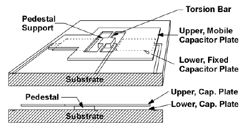
The accelerometer tells us which way the quadrotor is accelerating. This is useful because we can get an idea of how much the thing has moved by looking at acceleration over time (position is mathematically represented as the double integral of acceleration) so that we can move it back and keep it hovering on a steady position.
MEMS Accelerometer based on capacitive effects
A sonar is used to determine the distance from the sensor to an object. This helps in object detection an avoidance and is mostly used in fully autonomous quadcopters.
Ultrasonic Sonar sensor
All these sensors are connected to a microcontroller or other control circuitry to make the decision as to how to control the motors (and therefore the quadrotor itself) according to plan.
Depending on how autonomous you want it to be, one or more of these sensors are used in combination; sometimes more sensors are used or more processing is done on the signals to get more information about the environment: creating maps, computer vision and navigation systems.
The flight mechanics of the quadrocopter, as explained in the how it works section, are not that difficult, but a "design" limitation is the choosing of motor/propeller.
Choosing a motor/propeller combo (prop size and RPM: lift vs torque)
There's something about aerodynamics that is just way too complex for beginners to get a working understanding of in a few words, all the fluxes and stuff makes it hard enough that even designers of commercial propellers bunch a lot of things into "constants" or "factors" that they arrive at experimentally.
But generally, the importan stuff depends largely on two things: the effective area of the propeller and RPM (revolutions per minute).
Revolutions per minute are largely dependent on the motor, in fact, it is one of the parameters used in their marketing; usually expressed as Kv, RPM per volt applied.
The propeller is marketed in terms of diameter x "pitch". the higher diameter means higher area; higher pitch also means higher effective area because more of the propeller is pushing air to create lift.
Various propeller sizes and pitches
In choosing a motor/propeller combination, you have to figure out what you actually need or want out of the quadrotor:
A higher RPM of the propeller will give you more speed and maneuverability, but it is limited in the amount of weight it will be able to lift for any given power. Also, the power drawn (and torque required) by the motor increases as the effective area of the propeller increases, so a bigger diameter or higher pitch one will draw more power at the same RPM, but will also produce much more lift (meaning it will be able to actually lift more weight). [Torque is like the rotating power of the motor]
A slower rotating propeller is used when you have a motor that manages less revolutions but can provide more torque. In this case using a longer or higher pitched propeller (which uses more torque to move more air in order to create lift) will give you a similar lift to a higher rotating one of less length/pitch.
The choice depends on both motor availability and weight requirements.
Motor technologies: Brushed vs brushless motors
There's a debate regarding the use of brushed or brushed motor. First, a brief explanation of both:
Brushed motor
A brushed motor is your regular $1 toy car motor. They are called brushed because of the way the motor works: the direction of current in the rotating part (rotor) is changed using a mechanical switching mechanism, a pair of moving contacts called brushes disconnect from one side and connect to the other with every half rotation. This is done so the electric current keeps the rotor energized in such a way so as to keep being attracted to the permanent magnets, thus keeping it rolling.
Brushless motor inside view
A brushless motor is one where the commutation mechanism is outside the motor itself, most often electronic. The thing with brushless motors is that there are no moving parts in the electrical path of current, so it generates less electromagnetic noise as there are no sparks (which happens in brushed motors when the brushes disconnect and connect on the other side).
The debate goes about how brushless motors, with its fewer moving or parts, requires less maintenance and has higher performance for size and that brushed motors are "old", obsolete technology.
For the most part, the actual gains in performance come from the thermal characteristics of the motor: given the same power, a brushless motor will probably be smaller due to the fact that the heat dissipates through the mounting (remember, the windings are stationary and attached to the motor frame), a bigger motor. This means that for the same size motor, you can push much more current through a brushless to get more power.
Now here comes the big "but": since they have been around the longest, brushed motors have become very cheap to manufacture, which means prices are very low. Also, since the commutation in brushless motors is external, there's an added cost of buying and/or building the Electronic Speed Controller (ESC), which could cost as much or even more than the motor itself (which even on the lower range are more expensive than brushed motors), also with the increased complexity that comes with more components to deal with.
Brushed motors use a relatively simple speed control technique known as Pulse Width Modulation (PWM) that controls the effective power that the motor gets by quickly switching the power on and off.
So as you can see, there's a lot to dig into when working in quadrocopters. Next up, assembling our own quadrotor and the whole design process.
Any number of flip flops can be grouped together that share the same clock signal and work as a single unit. Common numbers of flip flops grouped together in a register are 4, 8, 16, and 32 (corresponding to 2^2, 2^3, 2^4 and 2^5).
A register functions as a more complete unit of memory within a circuit, grouping together data with a similar meaning in most cases, or just a more compact way of storing a bunch of bits. Most registers are made out of D flip flops due to the lower pin count needed for signals (JK would need much larger IC's because of the need for more control pins space).
There are four main kinds of registers, categorized by the way in which data is put in and taken out.
Parallel In, Parallel Out Registers
This kind is the simplest of registers. A parallel in/ parallel out is just a collection of flip flops that share a common clock signal but have independent data signals and outputs.
Their main application is storing data or state information (represented in binary digits) for use in later steps in sequential circuits.
Serial In, Parallel out Registers
Serial in/ parallel out registers get their input from a single data line. The output of the flip flop is used as one of the outputs, as well as connecting it to the data line of the next flip flop. What this accomplishes is that for every clock signal, the bits stored move one place and a new bit is captured at the first flip flop; the last flip flop is used just as another output, so its data is rewritten after every clock pulse.
This type of registers are used as buffers in digital data lines, where data is sent using only one wire but each bit is needed separately for further use.
Parallel in, Serial Out Register
Parallel in/ serial out registers have special control circuitry (sometimes a simple multiplexor suffices) that can select whether to use an external set of bits or the previous flip flop's output as input.
This is so that there's a possibility to get an external set of bits all at one (in parallel), and send them along one by one. Since each clock pulse the data moves to the next flip flop, the last can be used as the register's serial output, sending the data it stores one bit at a time.
In contrast to the receiving and "semimultiplexing" action of the serial in/ parallel out, the parallel in/ serial out combines number of data lines into a single one, most likely for transmitting over a digital line.
Serial in, Serial out Register
Kind of a special purpose register. This is always wired so that the first flip flop gets external data, and all internal flip flop's outputs are connected to the input of the next, the last one being used as output.
This register's main purpose is to delay the transmission of data in a digital data line.
Most situations need a counter that outputs only one value per transition, or in other terms, that all outputs change at the same time. In a ripple counter, when two or more bits need to change to reach the final output, intermediate outputs are generated, which can interfere with the correct function of other circuits that depend on the counter.
To overcome this limitation, the same clock signal applied to every flip flop to ensure that they all transition at the same time. The flip flop control signals now need some external logic to set them in the correct level for them to switch to the needed state.
The logic is simple: if all the previous flip flops are 1, then toggle the state (if 1, go to 0; if 0, go to 1). This is easily accomplished with an AND gate with N inputs where N is the number of previous flip flops, or its equivalent "cascaded" AND gates (one extra AND for every extra input, the output of a previous goes to an input of the next gate), which output will be connected to both J and K inputs in a JK flip flop, or adding an extra AND gate whose input is connected to the inverted output of the D flip flop.
The second flip flop is a special case, since there is only one previous flip flop to check, no logic is needed because it can be driven directly by the first flip flop's output.
Counters are one of the many applications of sequential logic that has a widespread use from simple digital alarm clocks to computer memory pointers. A counter is a collection of flip flops, each representing a digit in a binary number representation (which means each bit, depending on position, means a different number).
One of easier ways to build a circuit is to make a flip flop that controls the activation or switching of the second, and so on. This type of counter is called a ripple counter, since the switching signal propagates from one flip flop to the next as in a wave.
The Ripple Counter
For a simple ripple counter, JK flip flops with both inputs tied to 1 are the best option, since it will toggle state on the clock edge. For simplicity, the falling edge is used and assuming all flip flops start in reset state.
The first FF (Flip Flop) in the sequence gets the its input directly from the variable that needs to be counted. When it transitions from low to high to low again (this last transition generating a falling edge), in other words, when the input pulses, the FF changes to Set.
Since the First FF's output has not made a falling edge transition, the second FF remains Reset.
When another pulse appears at the input, the first FF changes to Reset again, creating a falling edge at its output, which triggers the second FF to transition to the Set state.
Another pulse, the first FF changes to Set; No falling edge at its output, the second FF keeps its state. Yet another pulse (Now four if you have been keeping the count), the first FF goes back to Reset, producing a falling edge; the second FF also goes back to Reset, producing a falling edge at its output that will trigger a third FF and making it Set.
If we assign the value of 1 to the first flip flop, 2 to the second and 4 to the third, we have a 3 bit binary number represented in there. Remember that with binary numbers, we add the values where the binary bit is set to 1.
As you can see, when all the transitions have occurred, the counter ends up with the count of input pulses it has received, representing them in a binary number.
The main drawback of this ripple counter is the fact that as the transition propagates from the first flip flop to the next, all the way to the last one, intermediate numbers are being set at the output, which introduces error and some confusion if a pure counter is needed.
This problem becomes most apparent when all the bits in the counter are set to 1 and another input pulse is applied: The output will be subtracted each time. In a 4 bit ripple counter, the max number that can be represented is 15 (1111), as the transition propagates, intermediate numbers 14 (1110). 12 (1100), 8 (1000) will appear before finally settling into 0 (0000).
The D flip-flop has some advantages over the standard latch, but there are some applications where the flexibility of extra control signals is just too much of an advantage to pass.
The transformation from simple RS latch to JK flip flop is done by connecting them in a Master-Slave configuration like the D flip flop, the non inverted output of the first latch to the Set input of the second, and the inverted output to the Reset.
At this point we still have just an edge triggered SR flip flop, meaning the forbidden condition is still there. To prevent it from happening, we extend the enabling logic of the first latch from a two input AND gate to a three input gate (or alternatively, connecting the output of the first and gate to one of the inputs at the second, and use the second output as the final output of the now three input gate).
The extra input is taken from the inverted output of the flip flop as a whole (the output of the second latch) for Set and the non inverted output for Reset. What this does is that when the flip flop is Set (output = 1) the Set connection gets disabled (negated output = 0) by since not all the inputs of the AND gate will be 1; This is done because if the Flip flop is already set, there's no point in "setting" it again, so that input can be disabled safely.
When the flip flop is Reset, the output will be 0 and disable the Reset input, since it cannot be "More Reset" than it already is, so it can be safely disabled.
What happens when both are 1 at the same time? Since the only time the output will change states is at one of the clock edges, and since at any point one of the inputs will be disabled, the output will depend only on the input that is active.
If the flip flop is Reset and both inputs are 1, only the Set input will be enabled. At the clock edge, the flip flop will be set.
If the flip flop is Set and both inputs are 1, only the Reset input will be enabled. At the clock edge, the flip flop will be Reset.
As you can see, The JK flip flop will toggle states when both inputs are 1, eliminating the forbidden state and its disadvantages while still maintaining the flexibility of multiple control signals.
This Flip Flop is called JK just to distinguish it from the RS latch and its forbidden combination; they work very similar, but the hazard free of the JK flip flop made it deserve a special name for itself.
There are several drawbacks with using the level gating approach, one of the most serious is the fact that during the time the enable signal is on, the control signals pass easily through the now transparent latch, causing every change in control signals to be passed along the output of the latch. This is of special concern when working with the bouncy contacts of a mechanical switch.
A good way to overcome this is by connecting two of these transparent latches in what is called a master slave configuration in which one latch is active during the high level of the enable signal and a second, which gets its input from the first, gets activated with the low level of the enable signal.
The latches themselves are not changed in any way, only the enable signal will be connected in a special way: the first gets the signal directly and the second gets an inverted version of it.
When the enable signal is low, the first latch is disabled by the control logic, so it holds its state (no change at the output). At the same time, the second latch is enabled by the inverted signal (~0 = 1) and so its output is the same as its data input, which is connected to the first latch. Since the first latch is not changing at this point, the output of the second latch will not change either.
The moment the enable signal goes high, the first latch is enabled and its input will be the same as its data signal due to the input logic used to overcome the forbidden combination. The second latch is at the same time disabled by the inverted enable signal (~1 = 0), so even when its data input changes due to the first latch changing its output, the final output of this configuration will not change.
As the enable signal falls back to a low level (goes to 0), the first latch gets disabled and holds the last bit of data it got, while the second now gets enabled and starts transferring its data input, which is connected to the output of the first latch, to its output. It is at this point where any data applied through the cycle gets its transfer to the final output of the circuit.
A master-slave latch, commonly known as flip-flop, is an edge triggered device, meaning that it will only perform its full function when the signal changes instead of using a signal level. In this example the D flip-flop is falling edge triggered, since the output only changes when the enable (or more commonly known as clock in edge triggered circuits) goes from high (1) to low (0).
So far we've been working with the same RS latch and all its limitations, such as the forbidden combination of inputs. By providing additional input logic and merging the control signals we have a more robust latch that is less prone to the unstable conditions of the simple RS latch.
For this new latch, the set and reset control signals are merged into one, the data signal. To control the flip flop with only one signal, we have to make sure that the latch is set when the data signal goes high (set to 1) and reset when it goes low (set to 0).
With only one signal this task is easily accomplished with an inverter gate. The non inverted signal will go to the set input and the inverted signal goes to the reset input. The enable circuitry goes after this new input logic to make sure that when the latch is not enabled it will maintain its current state, which would not be possible without this interface logic (one signal would always be high due to the inverter).
This simple arrangement of input logic combined with a two gate latch make it a very popular choice for high density Integrated Circuits (IC's). Sometimes the IC's whole memory and sequential logic is implemented using only latches very similar to these.
This circuit is called an SR latch because of its Set and Reset function and control signals.
A basic latch can be built with two NOR gates, with the output of one to one of the inputs of the other. The free input on both gates are used as control signals, one to SET the output to 1, and the other to RESET the output to 0. When no control signal is applied, the latch keeps its previous state via the conditions set at the output being fed back as inputs, which result in a condition that keeps the output the same.
The way in which the gates are wired make the output of one gate being the non inverted output of the latch, and the other being the inverted output.
There's one combination that will break that relation: when both Set and Reset are 1, both outputs will be at a 0 level. This in itself is not a cause for major concern, but when we make both control signals go from high to low at the same time, a race condition occurs.
This is called race condition because the output depends on which of the control signals stay high longer will determine the latch's output. If the set signal goes to 0 first, then the latch will have a 0 output (Reset), if the reset signal goes to 0 first, then the latch will have a 1 output (set).
The combination that produces this behavior is called a restricted or forbidden combination, because there's no way to actually know which signal will end up designating the latches output, which is not very good in a logic design where everything is supposed to be in one state or the other with full certainty.
This kind of latch is called a transparent latch because there are no synchronization or enabling signals, which means that the output will change as soon as the signals make it change; the latch doesn't restrict the flow of data through it.
Controlling the latch: Level Gated Latch
One way to have better control over the functioning of the latch, a layer of AND gates are connected between the control signals and the actual latch's gates inputs. One of the AND inputs is shared and is connected to a new control signal: the enable signal.
This new signal controls the availability of the set and reset inputs to the actual latch. When the enable signal is 0, no matter what the set and reset signals are, the latch will never receive them, only 0 will appear since it is connected at the AND gate's outputs, so it will only hold its previous state.
When the enable signal is at 1, the output of the AND gates will depend on the set and reset signals, essentially letting them pass through to the latch. As you can see, this new layer of gates and a new signal allow us to control whether we want the the latch to function (enable it) or to just keep its previous state (when enable = false [0])
This kind of enable mechanism is called level gating, since the control signals will only reach the latch when the gates it needs to pass are enabled by the level of the enable signal.
By using a circuit output as an input to itself so that the next output depends not only on the input signals that are applied at the moment but also on its current state (by feeding back the signal, which was in turn generated by a combination of previous inputs and outputs), we can create circuit that work in steps (sequentially).
To accomplish this we first need a subcircuit that will hold an output even if the inputs change. The most basic circuit that accomplishes this is called a latch.
Multiplexors are a simple combinational circuit whose function is to select one input line to pass to its only output, by selecting it using address/select lines, the number represented using the binary number system is the input that is being selected.
The input lines available often are a power of two (2, 4, 8, 16), and the number of select lines are the power to which 2 must be elevated to obtain the number of input lines (2^n = L, where n is the number of select lines and L is the number of input lines)
One way to look at the functioning of a multiplexer is that the select lines represent a row in the circuit's truth table, and the value connected to the corresponding input line is the output of that row, which will be passed to the final output of the multiplexer if that line is selected.
As you can see, this circuit can be used to implement an arbitrary truth table of n input variables (remember in the previous equation we used n to represent the number of select lines).
An advantage of this method over discrete gates in implementing a truth table is the fact that only one integrated circuit is used in practice, gates ussually needing more IC's because of lower integration (uses less gates per IC).
Boolean equations can also be implemented by first generating the truth table for it by evaluating the output variable for every possible input variable's value combination.
One disadvantage in using this method over discrete logic gates is the fact that since the multiplexer is not optimized for any particular configuration, so it tends to be slower in practice but such speed penalty affects only high speed and high gate count circuits.
Extending Quick Synthesis: ROM Logic Synthesis
The idea of using a somewhat generic circuit to implement any truth table without modifying the underlying circuit by using a multiplexor can be extended to the use of ROM modules in order to extend the number of input variables available (by having more address/select lines) and the number of outputs per combination (by having more output lines)
A ROM module is a type of memory circuit that is either built with its contents (Hardwired or Masked) or programmed (Programmable ROM). Each address selects a cell of memory (as opposed to a single line in the multiplexor) that contains the information to be passed to the output in groups of size that is a power of two (8 [2^3] and 16 [2^4] being the most common).
This allows us to implement simultaneous truth tables by programming each output line of each address as the output of one of those truth tables. It's basically like having many multiplexors connected to the same select lines, each implementing a different (or even the same) truth table.
Truth tables help determine the input combination that will yield a certain output value; This is useful when we want to translate a given truth table into a boolean equation that can be much easily manipulated and simplified before actually building a circuit, hopefully making the wiring eaasier and cheaper by using less components.
There are two complementary terms that we use to accomplish this: Minterms and Maxterms.
A minterm represents each row of the truth table that has an output of 1. To translate a truth table row into the corresponding minterm we AND (or multiply) each of the terms at the input, inverting (applying a NOT operator) to each variable whose state for that particular row happens to be zero.
For example, the three input truth table:
A B C Z
0 0 0 0
0 0 1 0
0 1 0 1 <---
0 1 1 0
1 0 0 1 <---
1 0 1 0
1 1 0 0
1 1 1 1 <---
The rows marked with an arrow represent the minterms of the table. The equation for this table would be
Z = (~A * B * ~C) + (A * ~B * ~C) + (A * B * C)
Note that all three minters go together in the same equation, since any of them can trigger an output 1 (if the first is true [1] OR [+] the second OR the third, the output is also true [1]).
Minterms are also called the sum of products representation because of the way they end up arranged in the equation.
Maxterms are the complementary operation of minterms. Maxterms are obtained from the rows that have a zero in them as output. Using the above example, all the rows not marked with an arrow are the table's maxterms.
To translate from the table to a boolean equation we OR (sum) each of the terms acting as input, applying a NOT operation to any input that happens to be a 1 for that particular row. Notice how the operation (AND for minterms, OR for maxterms) and the criteria for negation (when the input variable is 1 for minterms and when it is 0 for maxterms) are opposite of each other.
The equation in Maxterms for the example would be
Z = (A + B +C)*(A + B + ~C)*(A + ~B + ~C)*(~A + B + C)*(~A + ~B + C)
For this particular table, you can see that the equation in maxterms has more of them, this is because there are more 0's as output than 1's, and since each row having them is one term in the equation, the more there are the more terms the resulting equation will have.
The maxterm representation is also called a product of sums, because of the way they are arranged.
They are arranged in such a way because if any of them is 0, then the output should be 0 as well, even if the other terms are 1. This is because if one of the terms is 0, then it means that the combination of inputs matches one of the rows of the table that results in a 0 output, and no matter what the other terms are (any number multiplied by 0 is 0), the output should be 0 in order for the equation to work the same as what's specified in the table.
Aside from representing the functioning of a logic gate with a truth table and a grammatical (with words) definition, the use of logic equations can be used not only to represent logic gates and circuits, but also with the usage of some theorems and equivalences, to reduce the number of terms involved, simplifying the equation.
In logic equation every boolean variable involved is assigned a letter or symbol, very similar to the algebraic representation of unknown numerical values using letters; In fact, this approach to logic is called boolean algebra due to their similarity (remember that it is called boolean variables and algebra because of the person who did extensive work on the subject, George Bool).
Each input variable is usually assigned one of the first letters of the alphabet (A, B, C, and so on), and the output variables are assigned the last letters (W, Y, Z, and so on; note that X was specifically left out, this is because it is used as a "Don't Care" condition in logic simplification). This assignment of letters is arbitrary, any other letter or symbol can be used instead, but it is a common way to assign them and most people working in the area follow this pattern.
The logic operations are either written in uppercase (OR, AND, NOT) or represented by their logical symbol (V for OR, ^ for AND, ~ or the variable name overlined for NOT). Parenthesis are used to order the operations and force precedent evaluation before using in other operations, similar as in algebra where the operations in deeper levels of parenthesis are evaluated first.
For example, to represent the AND operation, using A and B as input variables and Z as output, you can write
Z = A AND B
or alternatively
Z = A ^ B
For a more complex circuit where the order is not always clear (similar to algebra, the evaluation is always left to right since there are no operations of higher priority like division or multiplication are in mathematical algebra), the use of parenthesis is encouraged, for example:
Z = A AND B OR B AND C
could mean very different things depending on how it is interpreted, so the equivalent form
Z = (A AND B) OR (B AND C)
being much more explicit in what gets evaluated first is preferred.
Another way to represent the operations in a logical equation is to simply use the mathematical operators that closely resemble their operations (+ for OR, * for AND); the NOT gate is an exception to this, as well as most compound gate. The only compound gates that have a symbol associated to them are the XOR gate (a + sign enclosed in a circle) and the XNOR gate (since it represents a logical equivalence, the = sign or the three line equivalence sign is used).
In order to graphically and orderly present each possible output from a logic gate or any digital circuit, a truth table is used. These tables present every possible combination of input states and its corresponding output.
The first columns represent each of the input variables, and the last one (or few if there's more than one) represent the output of the circuit. For low number of variables (lower than 4 or 5) the number of possible combinations is small enough to be able to represent in a truth table, and all possible input combinations and their corresponding output can be quickly visualized.
A logic system is one that anything it does can be translated to a true or false, present or absent, high or low, in other words, two opposite and contrasting states where the system can only be at one of them at any one time. Digital electronics use only two voltage levels to work with, one to represent a true, 1 or high (usually 3v or 5v) and another to represent false, 0 or low (a connection to ground, which is at 0v), which make the basis of any logic system.
But what does a true represent in a logic circuit? anything you can think of, it depends on what you are using it to model. One of the most used introductory digital systems is that of a car key alarm, where if the door is open while the key is still in the ignition, a buzzer alarm will sound alerting you not to let the key inside the car when you close it.
To construct a digital circuit for this alarm, you use one input to represent whether the door is open (will be true when it is open, false when closed) and another to represent whether the key is in the ignition (will be true when in the ignition, false when not). For this circuit we want the buzzer to sound when both conditions are true: the door is open and the key is in the ignition.
A digital system is not concerned if the key is only half in, at the on or off position or if the car is only half open or it didn't close correctly; all of these situations are either forced to one state of the other, or switching between both at a very high rate, but it must have one of only two values.
As you can see, we have modeled a fairly complex situation (an alarm controlled by a door and a key) to only two inputs that take only two values. This is what makes digital circuits very useful, they are dependable (a half closed door is an open door, just as a slightly open door).
Another method to create active filters using opamps is to create a voltage divider with a resistance and a reactance (from a capacitor). This approach has some advantages over the previously mentioned filters: they are easy to build, easy to understand, and have "programmable" gain.
In the reactive voltage divider, the input is applied to the non inverting input of the opamp. This is so that it can be used as a simple non inverting amplifier, the gain being set by extra resistors that do not interfere or need to be considered much in the filter's working; they are just there to set the amplifier feedback's gain.
The signal is applied in series with one of the components and taken at the input in parallel with the second. The choice of which component is in series and which in paralel with the non inverting input has direct consequences in the functioning of the filter.
If the series component is chosen to be a resistor, then the voltage at the capacitor will determine the signal to be amplified. Since the reactance of the capacitor gets lower with frequency, the higher the frequency the lower the signal available at the opamp input (remember the voltage divider formula: (Vin*R2)/(R1 + R2), in this case, it becomes (Vin*Xc)/(Xc + R) where Xc is the capacitive reactance); This configuration gives us a low pass filter.
With the capacitor being the series component, the voltage at the resistor now determines the signal available at the opamp input. As the frequency gets higher, the capacitor's reactance lowers, up to the point where it acts almost as just a wire; this means that the higher the frequency the more signal available to the opamp. This configuration gives us a high pass filter.
These two main types of voltage divider filters can be cascaded (The output of the first used the the input of the second) in a single stage (one opamp, multiple voltage dividers) or multiple stages (one opamp per voltage divider), the latter having better characteristics due to the opamp's compensating mechanisms.
Another variation of the opamp filter is the band stop or notch filter, called like that because it is as if you cut a notch in the frequencies that pass through the filter, allowing all frequencies outside the notch to pass and blocking the frequencies in that range.
Just as the high pass filter is a variation of the low pass filter, changing the reactive element from input to feedback, so is the band stop filter a variation of the band pass filter, but instead of changing components we are going to change the configuration of the components.
For this circuit, the input impedance consists of a resistor and capacitor in parallel (it was in series for the band pass), and the feedback impedance will be a capacitor and resistor in series (was parallel in bandpass). As you can see, only the connections change, the components stay the same.
At low frequencies, the input impedance is dominated by the resistor, since the reactance is much higher than the resistance (the connection is in parallel, the equivalent is always lower than the lowest value). At the same low frequencies, the feedback impedance is dominated by the capacitor's reactance, since it is also high compared to the resistor (the connection is in series, the equivalent is always higher than the highest value).
The gain of the opamp, connected in an inverting amplifier configuration, is given by -Zf/Zin. The input impedance Zin is very low, near by the input resistance, and the feedback impedance is very high, driven by the capacitors reactance; this makes the ratio very high, tending towards infinity by the increasing Zf at lower and lower frequencies (it is theoretically infinite at DC, or 0hz frequency).
One way to limit the gain, similar to what was done for the low pass filter is to use a resistor in series with either the whole feedback series connection or just across the capacitor. This makes the extremely high reactance of the capacitor not dominate at very low frequencies, instead the parallel connection is closer to the lower value, in this case the resistor. This is done to ensure that the opamp does not go into saturation, because if it does it clips the signal and distorts it.
At very high frequencies, the input impedance tends towards, since the capacitor acts as a very low value. With the feedback connection, the capacitor is also a very low value, but since there's the series resistor, the impedance will be limited to that value.
Looking at the gain equation (-Zf/Zin), you can see that the gain tends towards infinity, since the input impedance goes very low at high frequencies. To limit this, you can put resistor in series with the original parallel combination.
At intermediate frequencies, where the input impedance and feedback impedance are very close, the gain will be close to 1.
With all this, you can see that the notch filter is the opposite of the band pass filter: the band stop filter highly amplifies signals above and below the "notch" or middle frequencies, and doesn't amplify (instead of blocking) the intermediate frequencies. This is in contrast with the band pass that attenuated signals above and below, and also didn't amplify intermediate frequencies (gain of 1).
For all the filters discussed so far there are other far more efficient and that also block undesired signals and amplify the frequencies of interest.
When both types of filters are combined into one, that is, a capacitor and resistor in series is used as input and a capacitor and resistor are used in parallel for the feedback, a new type of filter emerges: the bandpass filter.
To see how this works, we need to simplify the circuit to use only one element instead of two, in order to make analysis easier. Since when AC is applied to a capacitor it can be replaced with its capacitive reactance in ohms, we can use that to combine it with the series resistor at the input, and with the parallel resistor for feedback.
This gives us an input impedance (Impedance is a generalization of resistance that also includes reactances, and is also measured in ohms) and a feedback impedance, in a configuration similar to the simple inverting amplifier.
Since both impedances are frequency dependent, the gain will be frequency dependent as well. At low frequencies, the input capacitor's reactance is very high and dominates the series combination with the resistor, so the input impedance becomes very large. At the same time, the feedback capacitor will also have a very high reactance, but this time the resistor dominates because the connection is made in parallel.
Since the gain is defined by the ratio -Rf/Rin, generalized to impedances as -Zf/Zin, where Z denominates impedances in most electronics literature. Since the feedback impedance is small, limited by the resistor, compared the input impedance which tends to infinity, the ratio will be very small and will attenuate the signal (Zf << Zin, so the ratio is less than 1). In this case, the extremely high input impedance drives the ratio towards zero.
At very high frequencies, the input impedance is dominated by the resistance, since the capacitor's reactance is very small. The opposite effect happens at the feedback, since now the capacitor dominates with its very low reactance, which makes the impedance very low.
Checking the gain ratio -Zf/Zin, we can see that now the input impedance is very low, limited by the input resistor, but the feedback impedance will be lower still, going towards zero, not being limited by anything since the capacitor is dominating the connection, so the ratio will again be very small, attenuating the signal. This time, the very small feedback impedance drives the ratio to zero.
At medium frequencies, where no single component dominates each connection, both input and feedback impedance will be very close to each other, since they will be a very similar value, assuming equal components. At the frequency where the series combination and the parallel combination have the same value, the gain will be 1, given by the ratio -Zf/Zin, where Zf = Zin; This is called the center frequency, and it is the only signal that will not be attenuated.
The overall effect is that this circuit will attenuate both high and low frequency signals applied to it, and only pass a small range (also called band) of frequencies where both input and feedback impedances have a very similar value, hence the name bandpass filter. This is useful when you need to block noise or extra signals created within a circuit.
For the differentiator, an input capacitor was used so as to block constant signals and just output the rate of change. Some examples of calculated derivatives where for constantly changing which resulted in a constant, and the sinusoidal wave which resulted in a cosinusoidal output, which is just a phase shifted sine wave.
To understand the differentiator's use as a high pass filter, we are going to focus on this last derivative and combine with our understanding of capacitive reactance.
Starting with DC and very low frequencies, the reactance of the capacitor becomes essentially infinite, since it blocks all current due to the voltage buildup inside of it. This makes the gain equation of the inverting amplifier it is based on to approach zero.
Vout = Vin (-Rf / Rin)
As the frequency increases, less residual charge stays in the capacitor making it less restrictive to the apparent current flow, which results in less reactance, driving the ratio of resistances higher as the reactance approaches zero.
At very high frequencies, the capacitive reactance becomes so low that it is essentially a closed switch, drawing large amounts of current that need to be compensated by the opamp, which reaches saturation on each semicycle of the input signal; At high frequencies the gain approaches infinity.
To limit the gain at high frequencies, a resistor is used in series with the input capacitor. What this does is that as the capacitive reactance gets lower to the point of approaching zero, the series resistance becomes the dominant component that prevents the flow of current, limiting the gain to the ratio of that input resistor and the output resistor, just like a simple inverting amplifier.
So you see, the differentiator also works as a high pass filter, being the inverse operation in both mathematical terms as the integrator (a derivative is the inverse operation of the integral) and in filter functionality (blocks the opposite side of the frequencies).
All circuits included here are recommended to be assembled in printed circuit boards. Printed circuit boards, or PCB's increase the circuit reliability and mechanical stability.